|
|||||||||||||||||||||||||||
|
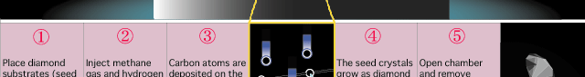
We conducted gemmological study on synthetic diamonds produced by CVD technique by Apollo Diamond Inc., and synthetic diamonds produced for research purposes by CVD technique by Element Six (De Beers Industrial Diamond Division). The stones we tested were type IIb of brown to near colourless, and it is usually very hard to distinguish these stones from natural diamonds only by common gemmological tests. However, their characteristic orange fluorescence under ultraviolet light and absence of anomalous double refraction due to strain called ügTatamiüh structure, which is commonly seen in type II natural diamonds, indicate their synthetic origin. Combination of laboratory techniques such as photoluminescence analysis (PL) and cathode luminescence analysis (CL) can identify between them clearly. ü¤ Introduction At the beginning of 1990s, synthetic diamonds became available on the gem market and then the new material became widely known to client in the industry. Most of the synthetic diamonds are typeIb with yellow colour and usually under 2ct weight, however, typeIIa of colourless and typeIIb of blue colour materials are also existence. In recent years, pink to red or purple colour stones have been produced by irradiation and heat treatment. Such stones have all been synthesized by high-pressure-high-temperature (HPHT) process and their identification method is based on the growth environment and crystal morphology that are essential to the HPHT process. According to Rapaport News, Apollo Diamond Inc. of Boston, Massachusetts in the United State announced in August 2003 its project to sell synthetic diamonds produced by CVD method for gem use. Apollo Diamond Inc. allegedly have developed technique to produce facetable high-quality CVD diamond over 2mm in thickness and the material is comparable in quality to rare natural typeIIdiamond. While the company has stated that it would fully disclose all the information, for instance, by inscribing on faceted products by laser, it also announced that the CVD diamonds, similar to HPHT treated diamonds, cannot be distinguished by standard gemmological instruments. Although CVD diamonds are not much paid attention by gem industry, researchers in recent years have already known that CVD method can produce high quality diamonds in several millimetre thicknesses. It is unlikely that CVD diamonds dominate gem industry right away. However, as Chatham Created Gems announced over ten years ago that it was going to sell synthetic diamonds produced by HPHT method and it lead us to the current situation, not only gemmologists but also all those who related to the gem industry should pay attention on the direction of development of CVD diamond hereafter. ü¤ What is CVD synthesis? Techniques to grow crystal by means of adsorption reaction and thermal decomposition of atoms and molecules contained in vapour are called vapour deposition methods. When this crystal growth process involves chemical reaction, it is called CVD (Chemical Vapour Deposition), and when a crystal grows physically, it is called PVD (Physical Vapour Deposition). In diamond synthesis process, when diamond, a crystal of carbon, is synthesised under high temperature and high pressure in which the diamond is thermodynamically stable, it is generally called high-pressure synthesis or high temperature high pressure method. Contrary to this, in CVD process, gas of organic compound such as methane containing carbon that is ingredient of diamond is dissociated in low temperature low pressure region (usually a tenth of atmospheric pressure), under which diamond is thermodynamically unstable, to make it into active status called radical, and then is deposited as diamond on a substrate maintained at between 800 to 1000 ºC. When the substrate is made of a single crystal of diamond (regardless natural or synthetic by HPHT method), a single crystal of diamond grows, whereas when the substrate is made of silicon, tungsten or molybdenum, polycrystalline diamond is produced. Quite large energy is required to activate the source gas, and there are several methods to do so, such as heating by filament (hot filament method), plasma heating by microwave (microwave plasma method), plasma heating by high frequency (high frequency plasma method) and heating by combustion-flame (combustion-flame method). Among these, microwave plasma method is suitable to synthesise high-quality single crystals in larger size (Figure 1) although it is not a successful CVD method to synthesise in large area.
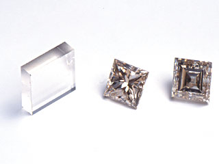
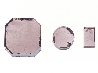
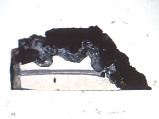
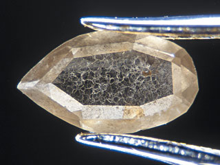
ü¤ Historical background In 1953, Eversole of Union Carbide Crop. in the United State proved that diamond showed homoepitaxial growth from carbon-bearing gas under low pressure. In 1956, Derjaguin of former Soviet Union announced that he successfully synthesised diamond by CVD method. In these methods growth rate of diamond was extremely low, and graphite also grew simultaneously with diamond so that in each case chemical reaction of the process had to be suspended. Fundamental research had been repeated thereafter and finally Matsumoto of NIRIM (the National Institute for Research in Inorganic Materials), Japan, made a breakthrough by succeeding development of a hot filament CVD method in 1981, followed by development of a microwave CVD method by Kamo of NIRIM. This method drew attention, as its experiment was reproducible and could produce crystals in good quality. On the 1st January 1986, major national newspapers reported an article of Mr. Hirose of Nippon Institute of Technology under the title ügDiamond made from Alcoholüh. This achievement sent messages to public widely that not only academic significance of the method but also the fact that diamond could be made from gas or liquid under low pressure. Compared to HPHT method, the CVD method uses small and simple device and it can be used for coating in any form with polycrystalline diamond, therefore it is expected to be applied to coating of machine equipment, heat sink of semiconductor equipment, window material for infrared and radial ray or to the electronics field. ü¤ Sample and method Nine pieces of CVD diamonds in total were used for this study. Three of them were produced by Element Six (De Beers Industrial Diamond Division) for research purposes, and were loaned by DTC Research Centre (Photo 1), two of which were square-cut brownish stones and the rest was nearly colourless, polished into tabular from rough. Element Six has launched research on the possibility of use of CVD diamond for gem purpose and on its detection since late 1980s. Another six pieces were produced by Apollo Diamond Inc., which were not for sale and we borrowed from Branko Deljanin of European Gemological Laboratory (EGL) (Photo 2). Among them four pieces were faceted but other two were rough as grown (Photo 3). The rest of the two had been HPHT treated to lighten the colour (Photo 4).
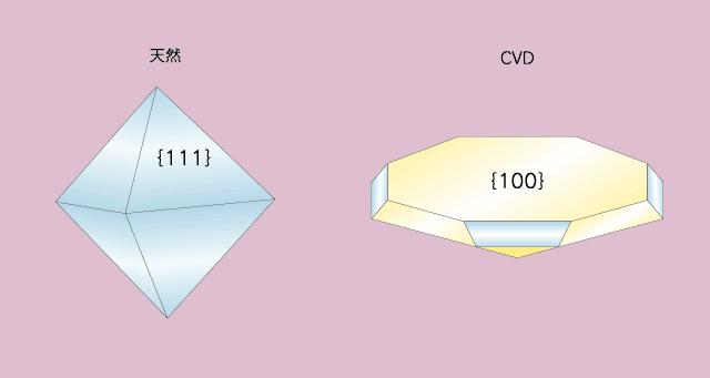
ü¤ Identification of CVD diamonds -Basic theory- Compared to HPHT method, a reaction chamber of the device for CVD method can be enlarged easily, and this means that the method may be developed as a synthesis of lager-size diamonds. However, it is difficult for this method to grow diamond in thick layer because its growth rate is extremely low. With the technique of early 1980s, it is calculated to take four months to grow diamond layer thick enough to obtain a 0.5ct brilliant cut stone, and six months for one carat. To solve the problem of growth rate, epitaxial growth has to carry out on a {100} substrate while retaining the condition (types and concentration of source gas and temperature of a substrate) to grow {100} face in preference to {111} face. From recent research, it is known that the growth rate can be accelerated by adding nitrogen gas, and it can achieve high speed growth rate of over 100ā╩m/h under a good condition. Such differences of growth environment between CVD diamond and natural diamond become key points to identify them, and the examples observed are different crystal morphology of diamonds grown in both environment and different impurity elements contained in those diamonds.
|
|||||||||||||||||||||||||||
|